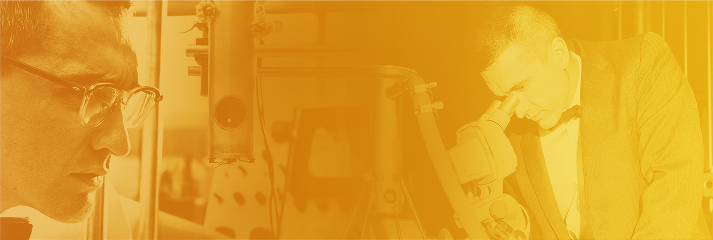
Prof. Nick Holonyak, Jr. received his B.S (1950), M.S (1951) and Ph.D. (1954) in electrical engineering from the University of Illinois. He was the first graduate student of Professor John Bardeen who later received two Nobel Prizes in Physics. Per Bardeen’s invitation, Dr. Holonyak returned to the University of Illinois in 1963 as Professor of Electrical and Computer Engineering where he remains today on the faculty doing active research.
He has mentored over 60 graduate students who have gone on to develop many useful semiconductor devices themselves. His work has led to over 575 papers and 51 patents. He is a member of the National Academy of Engineering (1973); National Academy of Sciences (1984); American Academy of Arts and Science (Fellow, 1984); Russian Academy of Sciences (Foreign Member, 1999).
He received the IEEE Edison Medal (1989) and the IEEE Medal of Honor (2003). He received the U.S. National Medal of Science (1990) and the U.S. National Medal of Technology (2002). He received the Japan Prize (1995), the Global Energy International Prize (Russia, 2003) and the Lemelson-MIT Prize (2005). He is a 2008 inductee to the National Inventors Hall of Fame. In 2015 he was awarded with the Charles Stark Draper Prize for innovative engineering achievement.
Nick Holonyak, Jr. is cited by most as the father of the visible light emitting diode (LED). His invention of the visible light (red) LED in 1962 at General Electric in Syracuse, NY initiated the broad use of III-V semiconductor alloy technology, enriching lives everywhere. The long-life red LED was initially used for panel indicators, traffic lights and automobile tail lights.
As other colors developed, applications broadened for low power illumination and decorative applications. LED lights produce the greatest amount of light for the energy used and have the longest lifetime of any lighting sources available. With the recent development of the white-light LED, a further option for long-life, low power illumination has become available commercially and is being marketed for general use. In the past few years we have seen many applications, now using incandescent or fluorescent lighting, being replaced with energy saving LED lights. The energy savings are of benefitworld-wide.
A key factor in Holonyak’s development of the visible LED was developing III-V semiconductor alloys such as gallium arsenide phosphide (GaAsP) which, with adjustment of alloy composition, can “tune” the semiconductor properties to a useful range. His work from 1960 to 1962 on GaAsP and the initial construction in 1960 of a p-n junction in this crystal system, and a visible-spectrum (red) laser in 1962, led to the commercial introduction of red GaAsP LED's and eventually to the concept of an "ultimate lamp". He is the inventor of the first practical light emitting diode (the GaAsP LED), which also marks the beginning in the use of III-V alloys in semiconductor devices (including heterojunctions).
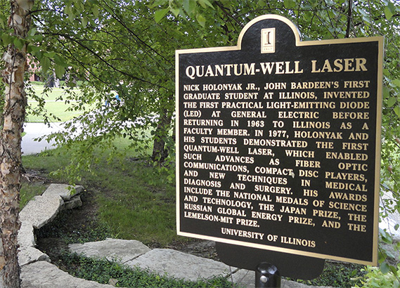
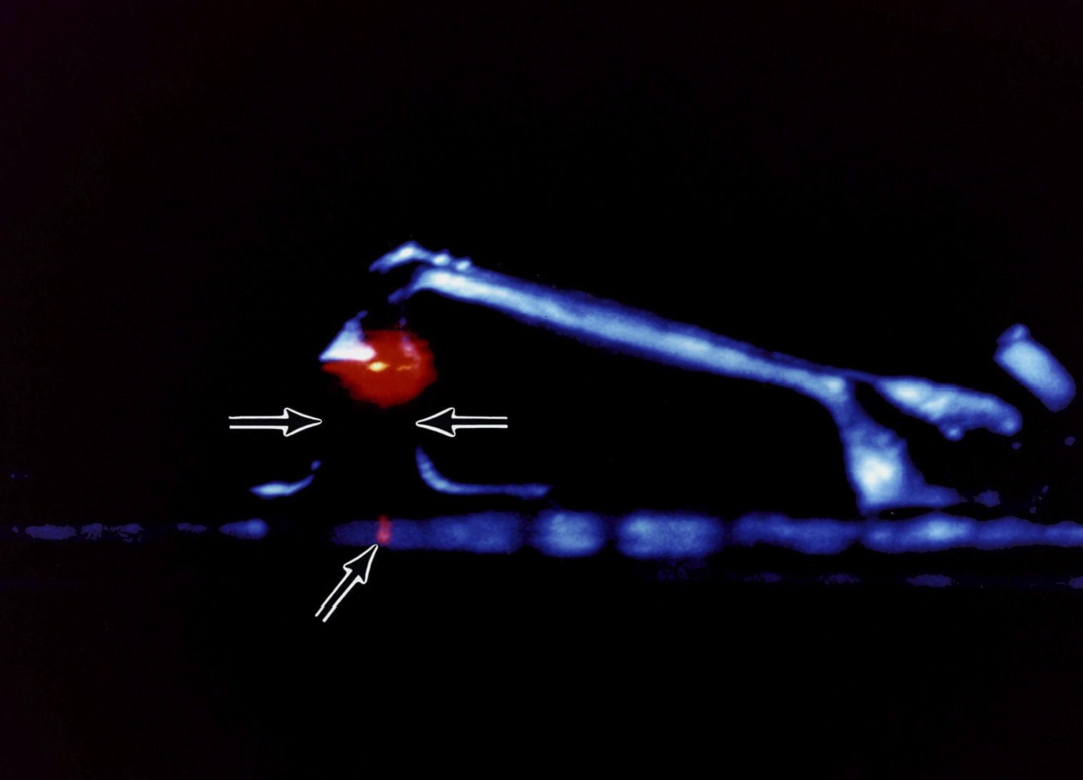
Late in 1977, Holonyak (with his student E.A. Rezek) developed the first quantum well (QW) semiconductor laser at the University of Illinois and also demonstrated in 1978 the first room temperature CW operation of a QW diode laser (with Dr. Russ Dupuis).
Today, every LED and semiconductor laser incorporates Holonyak’s work on III-V alloy semiconductors and quantum wells. These same alloys became the basis of a number of later inventions including other color of LED and the quantum-well diode laser commonly used for the read/write function on compact disks (CD) and later digital video disks (DVD).
In 1982, he discovered the impurity-induced layer disordering process, which shifts lower gap quantum well layers to higher gap bulk crystal and serves as a basis for integrated optoelectronic devices. The impurity-induced disordering proces sused on high power quantum-welldiode laser facets solved the reliability issues for a 980nm pump laser and is used in today’s undersea and long-haul communications (Dr. Don Scifres, SDL CEO).
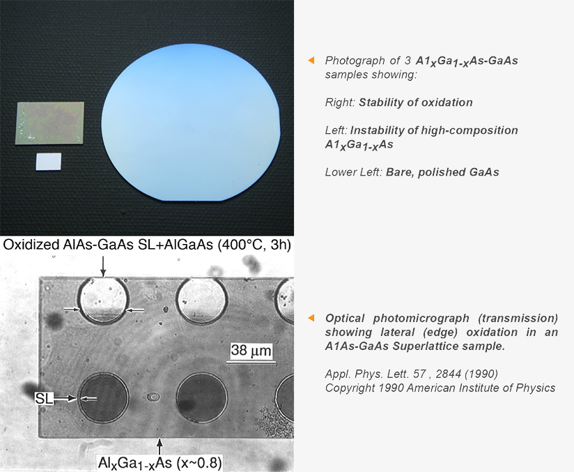
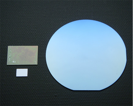
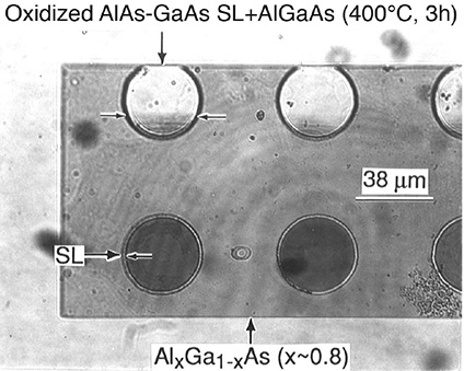
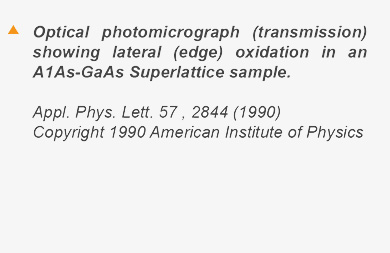
In 1990, Holonyak (with his student John Dallesasse) discovered (~ 400˚C) stable native oxides on, and buried in, Al bearing III-V compounds and demonstrated their use in optoelectronic devices (LEDs and lasers).
Today, every vertical cavity surface emitting laser (VCSEL) uses Holonyak’s oxide work for current and field confinement; the “Oxide-VCSEL” is the major high speed photonic source component used today in short-haul optical interconnects for super computers and optical networks.
Holonyak is currently working with Professor Milton Feng on advancing their 2004 transistor laser invention, the light-emitting three-port operation of heterojunction bipolar transistors, including QW-based HBTs and cavity, after 57 years, a transistor laser.
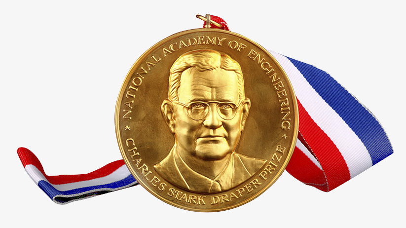
The Charles Stark Draper Prize for Engineering honors engineers whose innovative engineering achievements and their reduction to practice have led to important benefits and significant improvement in the well-being and freedom of humanity. Recipients recieve a commemorative medallion, a hand-lettered certificate and a $500,000 cash award.
The Prize was endowed to Prof. Holonyak by The Charles Stark Draper Laboratory, Inc., of Cambridge, Massachusetts, a pioneering nonprofit organization engaged in applied research, engineering development, education and technology transfer.